
Design For Assembly – Prevention of Solder Bridging in High Density Interconnect PCB Components
This is an advanced DFA technique developed by Cherie Litson in working with Microsoft engineers on the PCB design and manufacturing of the Microsoft Surface™.
11 September 2019 by John Walt Childers, founder of Golden Gate Graphics, a PCB design service bureau which operates out of both the Los Angeles and Denver metro areas.
I recommend that you first read Sam Sattel’s blog on “What Is Solder Bridging On a PCB?” (Google it to get there. A hyperlink to it did not function.) The technique described herein makes use of his “#3 – Use Solder Mask Defined Pads for Tight Pitched Areas.”
DFA Technique to Create 4-mil Solder Mask Dams between Adjacent PCB Lands
This write-up includes details of implementation in Altium Designer. It can most likely be used in just about any CAD package, but that is not guaranteed. Design for Assembly (DFA) is part of IPC’s DFX (Design for Excellence) initiative.
Use of proper solder mask defined pads helps the board house easily fabricate the PCB. A 4-mil solder mask dam between component pins helps the assembly house get better soldering results.
How does one keep both fabricators and assemblers happy and still get that 4-mil solder mask dam between landing pads of 0.5 mm or less pitch? (See additional note about PCB manufacturing at the end of this article.) I am referring to HDI (High Density Interconnect) components, either dual (two-sided) or quad (four-sided) packages with either formed leads or no-lead styles for their terminals.
Please make use of a glossary to help define technical PCB terminology.
A solder mask dam is a barrier between adjacent lands (also called landing pads) formed of solder mask.
Assembly houses want at least 4 mils of solder mask between landing pads. This helps prevent bridging of solder mask from one pad to another, which would be a short circuit.
4 mils (approximately 0.1 mm) is the narrowest solder mask sliver that is routinely manufacturable. Smaller than that can result in poor adhesion to the board and solder mask floating into the solder joint.
The technique described here requires knowledge of the actual dimensions of the terminals of the component.
Therefore, you will need the datasheet of the part. What you will want to know is the maximum dimensions of the metal terminal where it will contact the PCB. This means that footprints for the particular style of package might vary from one to another depending on the actual device used and its package dimensions and tolerances.
Steps to both Design for Assembly and also Design for Manufacturing
1. Build the footprint as usual.
2. Determine if it needs this solder-mask-defined-pad treatment.
3. Determine the maximum size and shape of the metalized terminals—the area where they will contact the PCB.
4. Use a special solder paste pad.
5. Make sure the copper lands have a size at least 2 mils larger than the solder paste pad all around.
6. Set the solder mask expansion to a negative amount so that it exactly matches solder paste pad.
7. Change the solder paste pads to rounded rectangles.
8. Give the footprint a new name to include the manufacturer’s case code.
9. Put a note on your Fabrication and Assembly specifications regarding the use of this technique.
1. Build the footprint as usual
Use rectangular pads. (You could also use oval or rounded rectangle pads, but this example is for rectangles.)

Basic_Footrprint_2D_SOTFL6P50_160X60L20W20
Red is copper, blue is solder mask object. Note that solder mask objects define an absence on the manufactured PCB of solder mask.
Fig 5-1 footprint name in IPC -7351C (pre-release) syntax is code for the following description: Small Outline Transisitor, Flat Lead, 6 pins, 0.5 mm pitch, body size is 0.16 X 0.6 mm and lead size is length 0.20 X width 0.20 mm.
The following drawing was contributed by Cherie Litson. This drawing represents a 0.40mm pitch QFN component.
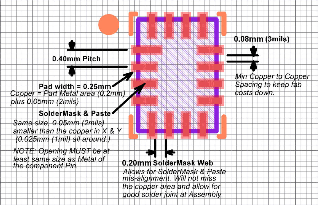
Design for Assembly – Design Rules for Solder-mask-Defined Pads of 0.40mm pitch Quad Flat No-lead component
2. Determine if it needs this solder-mask-defined-pad treatment.
To do this, carefully calculate the gap between the solder mask openings of adjacent lands. It should be at least 4 mils. If it isn’t, then continue with this technique.
Caution: If the pitch of the component terminals is 0.65 mm or more, you don’t need to use this technique. In this case, adjust the solder mask expansion of the pads. This can be as little as 2.5 mils and still be easily manufacturable by most board houses. If this solder mask expansion adjustment is not enough, make the copper lands narrower to bring the solder mask dam up to 4 mils.
Note also that many FFC connectors of 0.5 mm pitch won’t need this treatment because their terminals are narrower (typically 0.2mm) than dual and quad IC package terminals (0.27 mm max is typical). A terminal width of 0.2 mm leaves a space of 0.3 mm [11.8 mil] to work with. Subtract from that a minimal solder mask expansion (2X2.5 mil) and that leaves a solder mask dam of 6.8 mils. The copper lands can be oversized by 2.8 mils and still satisfy the 4 mil solder mask dam requirement (resulting in a land width of 10.7 mil [0.27 mm].
3. Determine the maximum size and shape of the metalized terminals—the area where they will contact the PCB.
For this example, the Texas Instruments’ case code DRL (R-PDSO-N6) is used. This is a flat-lead SOT package with 0.5 mm pitch.
I found the datasheet by Googling this case code. Here is a screen shot showing the terminal size.

Maximum terminal size is 0.4 X 0.27 mm
4. Use a special solder paste pad. Place pads on the solder paste layer exactly where the terminals will contact the landing pads.
This step is particular to Altium Designer. It may or may not be available in other CAD packages.
In most footprints, a special solder paste pad is not used. The solder paste opening is usually defined by paste mask expansion of the copper land, either negative, positive or zero. Zero expansion is the Altium Designer default. (Zero expansion means the solder paste stencil opening is the same size as the copper pad.)
To use a solder paste pad, you have to set this paste mask expansion of the copper land to be negative. Enough so that the paste mask expansion of the pad results in a smaller solder paste opening than the special solder paste pad. This forces the solder paste pad to be the controlling factor, thus overriding the paste mask expansion.

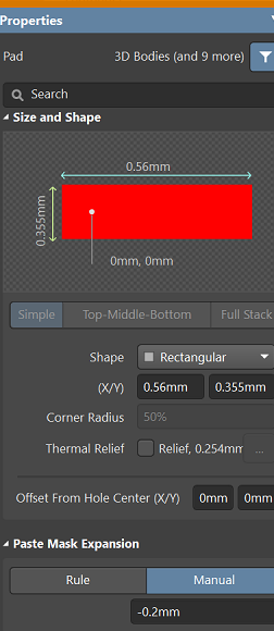
Solder paste pads Altium Designer
Colors: Red is copper land and tan is solder paste pad.
In the figure below, [Properties Panel—Paste Mask Expansion of Pad—SOTFL6P50_160X60L20W20_DRL (R-PDSO-N6)], the extra large paste mask expansion is -0.2 mm. You can see this number at the bottom of the panel.
These solder-mask-defined pads and solder paste pads must be the same width and at least as long as the metal terminals of the actual part. This size was determined in step 3, adjusted for toe and heel tolerances from the datasheet.
The size and locations are based on maximum limits of tolerance, not nominal dimensions. For the distance between the heels of opposite rows of terminals, the minimum is used. Thus you could have a solder paste pad and corresponding solder mask object that is longer than the maximum length dimension of the component terminal. Never smaller than the terminal.
 toe maximum and heel minimum")
DRL (R-PDSO-N6) toe maximum is 1.7 mm and heel minimum is 1.1 mm
In this datasheet, based on the 1.7 mm maximum toe-to-toe distance, minus the 1.1 mm minimum heel-to-heel distance, and then dividing by 2, the solder paste pad and the solder mask opening lengths of each land will be 0.3 mm. But the screen shot from the TI datasheet (Maximum terminal size is 0.4 X 0.27 mm) says the terminal length can be as much as 0.4 mm. I would use the larger of the two (0.4 mm, not 0.3 mm) and keep the heel-to-heel spacing at the minimum of 1.1 mm..
Drawing below is based on Cherie Litson’s white board drawing.

2016-03-13 4 Match Part Pin to Soldermask Opening
5. Make sure the copper lands have a size at least 2 mils [0.05 mm] larger than the solder paste pad all around
In other words, larger on both sides and toe and heel. This copper land will be at least 4 mils larger in width and length than the solder paste pad.
In the case of 0.4-mm-(or less)-pitch parts, this number will be decreased down to 1 mil all around.
Note that the toe of the copper pad can be longer as needed to match the data sheet recommended land pattern. A longer toe can also be useful on no-lead parts for providing a probe area for testing and debugging the prototype PCB. This longer toe won’t affect the 4 mil solder mask dam between lands.
Drawing is based on Cherie Litson’s white board drawing.

2016-03-13 5 Copper-to-Copper Clearance minimum 3 mils
6. Set the solder mask expansion to a negative amount so that it exactly matches the sides and heel of the solder paste pad.

2016-03-13 6 Solder Mask Negative Expansion Minimum 1 mil, Solder Mask Negative Expansion Nominal 2 mils, Solder Mask Dams at Least 4 mils, Pitches less than-half-mm require the minimums.

2016-03-13 6e BAD-Solder paste pads out-of-register with solder mask openings. (Colors: Solder mask is blue and solder paste is green.)
7. Change the solder paste pads to rounded rectangles.

Solder paste pads have rounded corners Altium Designer
Shown in draft mode. Colors: Red is copper land, blue is solder mask object and tan is solder paste pad.
This refinement was due to experimentation of the Microsoft Surface manufacturing team. It was found that if the solder paste stencil exactly matched the solder mask opening in size and shape, then the solder paste tended to peel up when the stencil was lifted. That is, the solder paste would adhere to the stencil instead of the printed board. Making the solder paste a rounded rectangle solved this problem.
If the assembly house uses an ink jet printer instead of a stencil to apply solder paste, this becomes a non-issue. If you don’t know which technique will be used to apply solder paste, it is safest to assume that a stencil is used.
If you chose to use oval or rounded rectangle pads, you can still modify the solder paste pad in order to prevent the solder paste from sticking to the stencil. In the case of a rounded rectangle copper pad, you would make the solder paste pad an oval. If you used the oval pad for copper, you would make the solder paste pad shorter than the solder mask opening.
8. Give the footprint a new name to include the manufacturer’s case code.
In this example, the footprint name started out as SOTFL6P50_160X60L20W20, which is an IPC-7351C*-patterned name. I changed the footprint name to add an underscore and Texas Instruments’ case code. Thus the footprint was re-named to SOTFL6P50_160X60L20W20_DRL (R-PDSO-N6). The reason for the extra information (the case code) is that it is possible that a footprint of the same IPC name would have different terminal sizes. Having the case code suffix in the name also tells me in a glance that I have given this footprint the solder-mask-defined pad treatment to achieve good solder mask dams..
* The publication IPC-7351 is the Generic Requirements for Surface Mount Design and Land Pattern Standard. The naming convention is one of the tables in the standard.
Version C of IPC-7351 has not been released. The format for IPC-7351C naming convention used here is from PCB Libraries, Inc., whose founder is Tom Hausherr. As part of IPC and beginning in 2001, Mr. Hausherr created the original IPC-7351 Naming Convention.
However, when IPC-7351C is finally released, it might be noticeably different from that as used herein.
9. One last thing – Be sure to put a note regarding use of this technique on your Fabrication and Assembly specifications
Specify that you have “SOLDER MASK DEFINED PADS” and the solder mask and paste mask should not be adjusted for manufacturing for these specific components/footprint names. You should detail which ones these are in your documents by referring to them by their reference designators.
That’s all there is to it.
Design for Manufacturing: Why PCB Manufacturers Don’t Like Identical Sizes of Copper Lands and Solder Mask Openings.
I have seen solder mask dams implemented by making the landing pad’s solder mask expansion equal to zero. This can give you a 4-mil solder mask dam in 0.5 mm-pitch footprints.
But it presents a problem for the board house. This situation creates neither solder-mask-defined nor non-solder-mask-defined pads. There is always a manufacturing tolerance. If it goes one way, the pad becomes solder-mask-defined, but if it goes the other way it is now a non-solder-mask-defined pad. It’s a compliance issue. The board house is required to comply with IPC standards and it can’t do that in this situation.
IPC Standards Don’t Include This DFA Technique. Yet.
Cherie Litson, being IPC CID+, an author of the IPC PCB Designer’s Certification Manual and an IPC master instructor, made the point to me that this technique is not an IPC standard at this time.
On the inside cover of every IPC manual, there is a statement on The Principles of Standardization. “In May 1995 the IPC’s Technical Activities Executive Committee (TAEC) adopted Principles of Standardization as a guiding principle of IPC’s standardization efforts.”
The Principles include this statement: “Standards should not inhibit innovation.” Therefore, I intend to continue to use this technique in my PCB designs.
Conclusion
For your HDI components, you can use PCB DFA and DFF (Design for Fabrication) techniques to create proper solder-mask-defined pads. The purpose is to create adequate solder mask dams between adjacent solder terminals.
Assembly houses appreciate any help in eliminating solder bridging.
Board houses will appreciate that it is done in a way that doesn’t cause problems for them.
Questions
Do you have questions about this technique? Please ask by posting a comment.
Have you had any complaints from your contract manufacturer about the data you provided them? Please post a comment.


Leave A Comment