

Altium Designer Official Service Bureau
Definition of Streamlined PCB Design
Streamlined PCB Design is a system for speeding design and build of printed boards. It is also a system for eliminating errors. However, it is not a quick-and-dirty way for a layout guy to make a fast buck. Therefore, some PCB designers have complained that it is more work for them, not less.
Streamline– v. Cause to be quick and efficient.
Altium Designer
Altium Designer works well in the Streamlined PCB Design system. There is advanced artificial intelligence built into Altium Designer. Therefore, one can use it to create expert control over design rules.
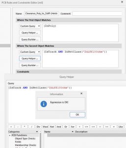
Altium Designer has advanced query features with Helper
Part of a PCB designer’s job in using a system like this is doing extra things to enhance the quality of PCB artwork. If one can assist the downstream actions in the overall production cycle, he has improved matters. Downstream actions that can be helped are board manufacture, assembly, test and repair.
Electrical Engineer
Upstream from the PCB designer is the electrical engineer, who is responsible for the circuit design. The PCB designer provides help in that direction in the form of feedback and questions.
Exchange
Streamlined PCB design leads to products (artwork and documentation) which get exchanged for money. Or within a corporate environment, it gets exchanged for goodwill and salaries and contributes to the corporation’s products which ultimately get exchanged for corporate income.
If one can eliminate whole categories of errors from creeping in, the overall cycle of production gets completed sooner with higher quality and reliability. Design and production become quick and efficient—streamlined.
“Streamlined PCB Design” is a set of policies that guide my design of printed circuit boards.
Error Elimination System
Eliminate all types of errors from creeping in and the overall cycle of production gets done sooner and with higher quality and reliability. Thus, you can cause design and production to become quick and efficient.
I use “Streamlined PCB Design” policies to guide my design of printed circuit boards. Frankly, these policies were borne out of a need to eliminate errors and omissions that I had been guilty of committing. I looked for and found ways to get rid of them.
Have you made mistakes in your PCB designs on occasion? What are some ways you have used to prevent such mistakes from repeating?


Leave A Comment